
Advanced Packaging

The Three-Headed Race in Advanced Packaging: TSMC, Intel, and ASE
Ethan Parker
For years, chip conversations revolved around transistor nodes and wafer fabs. Today, the more interesting battles are often happening a few millimeters above the silicon, in the world of advanced packaging. As AI, high‑performance computing, and high‑bandwidth memory redefine what a “chip” looks like, three names stand out in the packaging race: TSMC, Intel, and ASE. Each comes from a different starting point, with different strengths and weaknesses, and together they’re reshaping how heterogeneous integration will be done for the next decade.
Heterogeneous Integration of Silicon Photonics and Electrical Chips: CPO Commercialization
Ethan Richardson
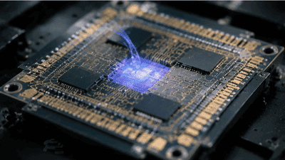
The semiconductor industry is entering a new phase where electrical interconnect alone is no longer enough. As AI clusters, data center switches, and high-performance networking platforms grow in scale, the old model of pushing more bits through copper traces is running into hard limits. That is where co-packaged optics, or CPO, comes in. By bringing silicon photonics and electrical chips into the same advanced package, CPO offers a practical path to higher bandwidth density, lower power consumption, and better scalability for the systems that move the world’s data.

ASE and Amkor’s 2026 CapEx Priorities – Advanced Packaging Focus
Ethan Brooks
If 2025 was the year the market finally accepted that advanced packaging was no longer a niche, 2026 is the year ASE and Amkor are acting like it. Both companies are putting capital behind the same big idea: advanced packaging and heterogeneous integration are now central growth engines, not side businesses. The scale of their spending plans says as much as any earnings call or roadmap slide. In a market reshaped by AI, HPC, chiplets, and HBM, CapEx has become a statement of strategy.

Power/Signal Integrity Simulation Challenges in MCMs
Charles Foster
Multi-chip modules, or MCMs, have become one of the most practical forms of advanced packaging and heterogeneous integration. Instead of forcing every function onto one die, designers can place several dies side by side in the same package and connect them through an interposer, substrate, fan-out structure, or other high-density routing fabric. That flexibility is powerful, but it also creates a new class of simulation problems. Power integrity and signal integrity, once mostly chip- or board-level concerns, now have to be solved inside a tightly packed multi-die environment.

Upgraded EMC Material Requirements in Advanced Packaging
Jonathan Mercer
Advanced packaging has changed the way semiconductor systems are built, and with that change has come a quieter but equally important evolution in materials. One of the most overlooked heroes in the entire stack is EMC, or epoxy molding compound. In simple packages, EMC was mostly a protective shell. In advanced packaging and heterogeneous integration, it has become a structural, thermal, mechanical, and reliability-critical material that helps make the whole system viable.

CoWoS Packaging Capacity Doubles in 2026, Yet Supply Gap Remains
Christopher Morgan
In 2026, the semiconductor industry hit a milestone that would have seemed ambitious only a few years ago: the global capacity for chip-on-wafer-on-substrate, or CoWoS, advanced packaging roughly doubled. By any traditional metric, that should have eased the pressure on cutting-edge compute supply. Yet, in practice, the opposite is happening. Despite this dramatic expansion, demand for CoWoS capacity still outstrips supply, and the gap is reshaping strategies across the semiconductor ecosystem.

Competitive Landscape of Advanced Packaging: The Coopetition Between OSATs and Foundries
Benjamin Harris
Advanced packaging has moved from the back end of semiconductor manufacturing to the center of the industry’s strategic map. As AI, high-performance computing, mobile systems, automotive electronics, and chiplets all push toward heterogeneous integration, one question has become unavoidable: who owns the packaging layer of the future, OSATs or foundries? The answer is not a clean winner-takes-all outcome. It is a complex and evolving contest of overlap, specialization, and cooperation. In other words, it is cooptition.

New Standards for Cleanroom Grades and Environmental Requirements in Advanced Packaging
Charles Wilson
Advanced packaging has changed the rules of semiconductor manufacturing, and cleanroom standards are changing with it. What used to be a largely front-end concern is now a packaging concern too, because heterogeneous integration depends on much more than just transistor quality. It depends on the cleanliness of bonding surfaces, the stability of thin wafers, the behavior of mold compounds, the integrity of fine-pitch interconnects, and the control of particles, humidity, and temperature throughout assembly. In short, the environment has become part of the design.

Surging Demand for Laser Drilling and Plasma Dicing Equipment in Advanced Packaging
Andrew Wilson
Advanced packaging has become one of the semiconductor industry’s most important growth engines, and it is now pulling a surprising set of process tools into the spotlight. Among the most in-demand are laser drilling and plasma dicing equipment. These machines sit close to the heart of heterogeneous integration, fan-out packaging, wafer thinning, TSV formation, glass substrate processing, and other advanced flows where precision, yield, and throughput matter enormously. As packaging moves from a back-end afterthought to a strategic platform, the equipment used to shape, open, and separate materials has become just as important as the dies themselves.
Chiplet Ecosystem Standardization: UCIe Alliance’s 2026 Milestones
Nathan Foster
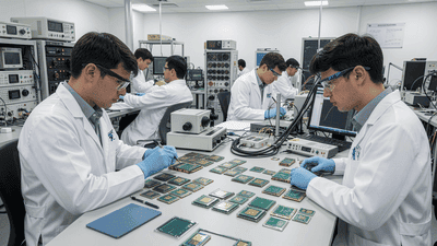
By 2026, it has become clear that the future of advanced encapsulation and heterogeneous integration will be defined as much by standards as by process technology. Universal Chiplet Interconnect Express, or UCIe, sits at the center of this transformation. Launched as an open die-to-die interconnect specification for chiplets, the UCIe Alliance has now accumulated several generations of specifications and ecosystem deliverables that are reshaping how the industry thinks about system design, advanced packaging, and multi-vendor chiplet interoperability.

Domestic Substitution Space for Advanced Packaging Materials (Underfill/TIM)
Ryan Mitchell
As advanced packaging and heterogeneous integration move from niche capabilities to mainstream semiconductor strategy, materials that once lived quietly in the background are suddenly in the spotlight. Underfill and thermal interface materials, or TIMs, are especially important. They are not glamorous, and they rarely make headlines, but they influence yield, reliability, and thermal performance in some of the most demanding packages being built today. That is why the domestic substitution space for these materials is becoming such a major topic.
New ATE Requirements from Advanced Packaging: From Single Chip to System-Level
Samuel Bennett
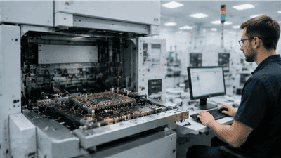
Advanced packaging has changed what it means to test a semiconductor device. For years, automatic test equipment, or ATE, was optimized around a simple idea: validate one chip, one die, one set of pins, one set of failure modes. That world is fading fast. In its place is a much richer and more complicated one, where the “device” under test may be a multi-die package, a chiplet-based module, a 3D stack, or a heterogeneous system built from several process nodes and several vendors.

Hybrid Bonding Transitions from Lab to Fab: 2026 Application Nodes
Alexander Morgan
In 2026, hybrid bonding is crossing a critical threshold: it is no longer just an impressive lab demonstration, but a production-ready enabler for advanced encapsulation and heterogeneous integration. Over the last decade, research consortia, equipment suppliers, and IDMs have steadily refined hybrid bonding processes, addressing alignment, contamination, yield, and reliability challenges. Now, a growing list of products in logic, memory, and mixed-signal domains are starting to rely on hybrid bonding at real application nodes, not just at experimental test vehicles.

FOWLP Penetration in Mobile AI Chips
Thomas Walker
Walk into any flagship smartphone launch in 2026 and you will hear three phrases on repeat: on-device AI, power efficiency, and thin design. Hidden behind those buzzwords is a quiet hero in the supply chain: fan-out wafer-level packaging, or FOWLP. Once a niche technology for RF and power management ICs, FOWLP is rapidly finding its way into the heart of mobile AI chips, becoming a key enabler for the performance and form factors consumers now take for granted.

Reliability Testing of Hybrid Bonding Interfaces in 3D-Stacked Memory and Logic
Adrian Mitchell
Hybrid bonding has become one of the most important enablers of advanced packaging and heterogeneous integration. It allows memory and logic dies to be joined with extremely fine pitch, low interconnect resistance, and a level of vertical density that traditional micro-bumps cannot match. That technical promise is exciting, but it also raises a hard question: can these interfaces survive real-world operation for years, under heat, stress, and repeated power cycling? Reliability testing is where the answer is found.

Advanced Packaging’s Share of Total AI Chip Cost Exceeds 30% for the First Time
Thomas Walker
For the first time, advanced packaging now accounts for more than 30% of the total cost of leading AI chips. What used to be a small, back-end line item has become one of the largest cost buckets alongside high-bandwidth memory and wafer fabrication. This shift is not a statistical curiosity; it is a structural turning point in how AI hardware is built, priced, and constrained. Advanced packaging has moved from the periphery of the semiconductor value chain to its center.

The Advanced Packaging Revolution: Glass Core Substrates vs. Organic Substrates
Lucas Bennett
Walk into any discussion about next-generation AI accelerators or high-performance computing today and you will hear something that would have sounded odd a decade ago: people are arguing about substrates. Not just about die size or node technology, but about what sits under the silicon – glass core substrate or traditional organic substrate. That debate captures a quiet revolution in advanced packaging and heterogeneous integration, as the industry tries to stretch system-level performance without relying solely on transistor scaling.

Panel-Level Packaging (PLP) vs. Wafer-Level (WLP): The Cost Battle
Richard Evans
Advanced packaging has become one of the most important battlegrounds in semiconductors, and nowhere is that clearer than in the contest between panel level packaging and wafer level packaging. Both approaches aim to make packages smaller, denser, and more capable of supporting heterogeneous integration, but they do so with very different economics. That is why the PLP versus WLP debate is not just a technical comparison; it is a cost battle that will shape which applications scale fastest in the years ahead.
2027 Advanced Packaging Roadmap: From 3D SoIC to Co-Packaged Optics
Lucas Anderson
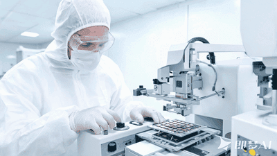
The 2027 advanced packaging roadmap is shaping up to be less about a single breakthrough and more about a sequence of tightly linked transitions. On one end sits 3D SoIC, a powerful expression of vertical integration that pushes logic and memory closer together than traditional packaging ever could. On the other end sits co-packaged optics, or CPO, which aims to move the bottleneck of data movement out of electrical interconnect and into the optical domain. Between them lies the broader world of advanced packaging and heterogeneous integration, where chiplets, HBM, hybrid bonding, fan-out, and new substrate technologies are converging into a new system architecture playbook.
Domestic Progress of Advanced Packaging Tools (Bonders/Molders/Grinders)
Ryan Mitchell
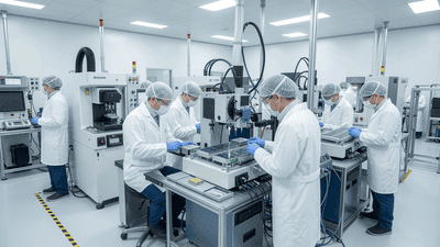
If you want to understand how serious a country is about advanced packaging and heterogeneous integration, do not just look at its wafer fabs. Look at its bonders, holders, and the investors behind them. Those quiet, often overlooked tools and capital flows tell you whether the ecosystem is really ready for 2.5D and 3D integration, chiplets, HBM, and all the other buzzwords of the AI era—or whether it is still just talking about them.

2026 Forecast of China’s Advanced Packaging Capacity as a Global Share
Andrew Wilson
China’s role in advanced packaging is moving from “important participant” to “strategic balancing force” in the global semiconductor supply chain. By 2026, its capacity is expected to represent a meaningful share of worldwide advanced packaging output, especially in high-volume OSAT-driven segments, even as some of the most cutting-edge AI packaging still remains concentrated elsewhere. That contrast is exactly what makes the story interesting: China is scaling fast, but the global market is not all one market. Different packaging technologies, different end markets, and different levels of localization are expanding at very different speeds.
D2D Interface Bandwidth and Latency Comparison in Chiplet Architectures
Daniel Morgan
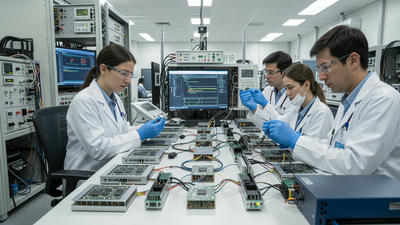
Chiplet architecture has turned the package into a real performance battleground. Once multiple dies are placed side by side or stacked within the same advanced package, the quality of the die-to-die, or D2D, interface becomes one of the most important determinants of system behavior. Bandwidth is no longer a nice-to-have metric, and latency is no longer a small implementation detail. Together, they shape whether a chiplet system feels nearly monolithic or frustratingly fragmented.

Thermal Management in Heterogeneous Integration: Embedded Microfluidic Cooling Solutions
Ethan Parker
Anyone who has opened a laptop after a long gaming session knows that heat is the silent enemy of electronics. Now imagine that same problem in a package holding multiple high-power chiplets, stacked dies, and dense memory, all squeezed into a few square centimeters. That is the world of heterogeneous integration—and it is brutally hot. Traditional cooling methods are being pushed to their limits, and that is where embedded microfluidic cooling starts to sound less like a futuristic research topic and more like a practical necessity.

Value Distribution of Advanced Packaging via AI Chip Teardown Analysis
Robert Carter
If you want to understand where the real value sits in modern AI hardware, teardown analysis is one of the best tools available. Once you open up a flagship AI accelerator and examine its layers, you quickly discover that the package is no longer a supporting actor. It is a major source of cost, performance, and strategic value. In many cases, advanced packaging now accounts for a surprising share of total device value, rivaling or even surpassing the logic die in importance once HBM, interposers, substrates, and assembly are included.

The Critical Role of Silicon Interposers in Large-Size AI Chips
Henry Cooper
When people talk about the future of AI chips, the conversation usually starts with transistor nodes, model sizes, or memory bandwidth. But behind all of that sits a less glamorous, yet absolutely decisive, piece of technology: the silicon interposer. In large-size AI chips, the interposer is what makes heterogeneous integration practical at scale, tying together massive compute dies, multiple HBM stacks, and increasingly complex chiplet ecosystems into one high-performance package.
Warpage Control in Advanced Packaging: The CTE Matching Challenge
Andrew Wilson
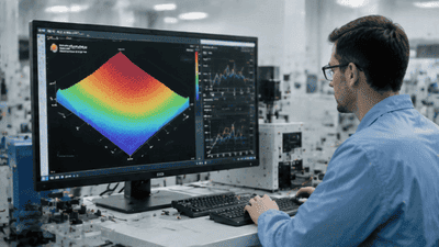
Advanced packaging has made semiconductor systems more powerful, denser, and more flexible than ever, but it has also exposed a stubborn mechanical problem that refuses to go away: warpage. As heterogeneous integration pushes more dies, more layers, and more materials into a single package, the question of how those materials expand and contract becomes central to yield, reliability, and manufacturability. At the heart of that problem is coefficient of thermal expansion, or CTE, matching.

Techno-Economic Comparison of 2.5D vs. 3D Packaging: Which to Choose When?
Charles Wilson
Advanced packaging has become the place where semiconductor scaling is now negotiated, and two of its most important options are 2.5D and 3D packaging. Both are powerful forms of heterogeneous integration, but they solve different problems, carry different risks, and make sense at different points in a product roadmap. The real question is not which one is better in the abstract. It is which one gives the best balance of performance, cost, yield, thermal behavior, and manufacturability for a specific system.

New EDA Challenges and Tool Iterations Driven by Advanced Packaging
Richard Evans
Advanced packaging has changed the semiconductor design flow in a way that feels subtle at first and then suddenly unavoidable. What used to be the back end of the line—package selection, assembly, and test—has become a co-equal design domain alongside logic, memory, and interconnect. As heterogeneous integration moves from a niche practice to the default architecture for high-end AI, HPC, networking, and mobile systems, EDA tools are being pushed far beyond their traditional boundaries.

TSV Cost Structure and Yield Ramp-Up in 3DIC
William Brooks
Through-silicon via, or TSV, technology sits at the heart of many advanced packaging and heterogeneous integration roadmaps. As the industry moves from 2D scaling to 3D integration, TSVs enable vertical stacking of dies, shorten interconnects, raise bandwidth, and improve system performance. Yet behind the impressive technical benefits lies a complex story of cost structure, yield ramp, and manufacturing learning curves that determine how quickly 3DIC can become mainstream in high-volume production.

2026 Global Advanced Packaging Market Exceeds $60B – Supply Chain Breakdown
Andrew Cooper
The advanced packaging market has entered a new phase. In 2026, global revenue is expected to exceed $60 billion, a scale that would have seemed surprisingly high only a few years ago. What changed is not just demand, but the nature of demand itself: AI accelerators, high-bandwidth memory, chiplets, and heterogeneous integration have turned advanced packaging from a niche technology into a core growth engine for the semiconductor industry. The headline number is impressive, but the real story is the supply chain underneath it.