
Materials

Sputtering Target Material Transition: Al, Cu, Ti, and Co in Advanced Interconnects
Adrian Mitchell
The wiring inside a semiconductor is becoming as important to performance as the transistors it connects. As features shrink, moving electrical signals through narrow lines and tiny connections becomes increasingly difficult. Resistance, reliability, and manufacturing consistency turn metallization into a materials-engineering challenge.

High-Purity Quartz Supply Risk: The Monocrystal Pulling Bottleneck
Benjamin Harris
The semiconductor industry usually describes its vulnerabilities through familiar headlines: lithography restrictions, advanced packaging shortages, scarce photoresists, or interruptions in specialty gases. Yet one of the most consequential dependencies sits much earlier in the manufacturing chain. Before a silicon wafer reaches a fabrication plant, its crystal must be grown. For much of the industry, that means pulling a single crystal from molten silicon held inside a quartz crucible.
Photomask Localization: Qingyi and Luwei’s Progress
George Anderson
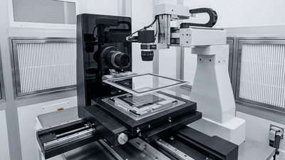
China’s semiconductor localization story is often told through fabrication equipment, silicon wafers, photoresists, and specialty gases. Photomasks receive less attention, despite occupying a decisive position in manufacturing: they carry the patterns that lithography transfers onto a wafer. Without a suitable mask, a qualified process cannot turn a circuit design into repeatable production.

Precursor Demand in ALD and CVD: The Korean Supplier Dominance
Henry Cooper
A semiconductor’s most important materials are not always visible in the finished device. Some arrive at the factory inside specialized containers, enter a deposition chamber as vapor, and disappear into films only a few nanometers thick. These precursors help form the insulating layers, electrodes, barriers, and other structures that allow modern chips to operate.

Wet Chemicals G5 Purity: The Domestic Qualification Breakthrough
Ethan Parker
A semiconductor fabrication plant can install advanced equipment, secure high-quality silicon wafers, and develop sophisticated process recipes, yet still lose performance to contamination carried by an ordinary-looking liquid. Sulfuric acid, hydrogen peroxide, hydrofluoric acid, and ammonia solutions appear unremarkable beside a lithography scanner. Inside the fab, however, their cleanliness can influence whether a carefully engineered surface survives the next manufacturing step.

CMP Slurry Advances: Dinglong’s Cerium Oxide and TSV Polishing Wins
Ethan Richardson
The semiconductor supply chain has a habit of hiding its most consequential dependencies behind its least glamorous materials. Advanced lithography attracts headlines. AI accelerators attract capital. Yet before a chip can become either a technological breakthrough or a commercial success, it needs a wafer—and most mainstream silicon wafer production depends on growing a single crystal inside a quartz crucible.

Electronic Specialty Gas Demand from Advanced Nodes: The Localization Acceleration
Edward Collins
Semiconductor manufacturing is often described through its most visible assets: lithography machines, cleanrooms, silicon wafers, and increasingly expensive fabrication plants. Yet some of the materials that determine whether those investments produce usable chips arrive through pipes and cylinders. Electronic specialty gases belong to this less visible but strategically important layer of the industry.

Photoresist Pricing: Shin-Etsu and JSR’s China Strategy Shift
William Turner
Photoresist pricing has become a revealing lens through which to examine the changing relationship between Japanese materials suppliers and China’s semiconductor industry. For a wafer fab, photoresist is a recurring procurement item. For a process engineer, it is a carefully qualified component of a manufacturing recipe. For a supplier such as Shin-Etsu Chemical or JSR, it represents a combination of chemical expertise, customer integration, and commercial leverage.
Semiconductor Material Hidden Champions: The Small-Cap Opportunity Map
Christopher Morgan
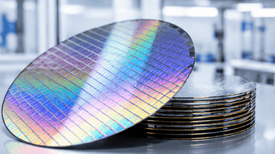
The semiconductor market rewards visible products: accelerators, memory, leading-edge manufacturing, and the equipment that makes them possible. Far less visible are the materials that allow those operations to run consistently. A wafer, photoresist formulation, specialty gas, or sputtering target may attract little attention until its quality or availability becomes a production problem.

Silicon Wafer Shipment Area Growth: The 2026 Recovery Trajectory
Daniel Morgan
The silicon wafer market is recovering in 2026, but the recovery is neither uniform nor adequately explained by the artificial intelligence investment boom alone. Shipment area is increasing, advanced applications remain the strongest demand engine, and industrial and automotive markets are showing signs of improvement. Yet rising volumes do not automatically imply stronger pricing, fully utilized factories, or an equally healthy outlook across wafer categories.

Wafer Edge Polishing Equipment: The SOI Substrate Demand Driver
Daniel Brooks
The center of a semiconductor wafer receives most of the attention. That is where engineers measure film thickness, pattern devices, and evaluate electrical performance. The edge looks less productive: a narrow perimeter that cannot accommodate complete dies and often sits outside the usable processing area.
Advanced Packaging Material Demand: Underfill and TIM Localization
Nathan Collins
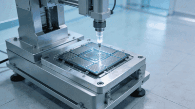
A large AI package can contain exceptional silicon and still fail because a relatively inexpensive material does not behave as expected. An underfill that leaves voids can compromise interconnect reliability. A thermal interface material that loses contact can turn an acceptable cooling design into a temperature problem.

2026 Global Wafer Shipment Area YoY Growth Forecasts: Divergence and Consensus
Oliver Bennett
As the semiconductor industry moves through 2026, expectations for global wafer shipping area growth sit at the core of many strategic decisions. Year‑on‑year (YoY) wafer area forecasts influence how wafer manufacturers plan capacity, how fabs schedule expansions and technology migrations, and how equipment and materials suppliers shape their own production plans. Yet the forecasts themselves are far from uniform. Different institutions—industry bodies, market research firms, banks, and corporate strategists—offer projections that diverge meaningfully in magnitude and composition, even when they point in broadly similar directions.

Shelf Life and Inventory Management of Semi Materials – A Test of Supply Chain Resilience
William Parker
The semiconductor industry is one of the most sophisticated manufacturing ecosystems in the world, relying on thousands of materials with extremely strict quality requirements. From silicon wafers and photoresists to specialty gases, electronic chemicals, and packaging materials, every component must meet precise specifications to ensure stable semiconductor production.

Rising LTA Coverage of Wafer Giants – A Stabilizer for Industry Profitability
Matthew Collins
In the complex and cyclical world of semiconductors, stability is a scarce resource. Demand for chips fluctuates with consumer trends, enterprise investments, and macroeconomic swings, while supply chains stretch across continents and multiple tiers of specialized suppliers. Amid this volatility, one segment has become a quiet anchor for industry profitability: the long-term agreements (LTAs) signed between major wafer suppliers and their customers. As LTA coverage rises among wafer giants, it increasingly acts as a stabilizer, smoothing financial performance for both wafer makers and fab operators and reshaping how risk and reward are shared across the value chain.

Qualification Cycles for Domestic Semi Materials Shorten from 24 to 12 Months
Andrew Mitchell
In semiconductor manufacturing, material qualification has traditionally been a long and cautious process. For many critical inputs—wafers, gases, wet chemicals, photoresists, CMP consumables, packaging substrates—domestic suppliers often faced qualification cycles of 18–24 months or more before their products could be used in high‑volume lines. Now, in multiple regions, those cycles are shortening, with leading fabs moving toward 12‑month or even sub‑12‑month qualification for carefully selected domestic materials. This shift reflects both greater confidence in local suppliers and strong strategic pressure to accelerate localization without compromising quality or reliability.
SiC Substrate Cost Reduction Curve – Poised to Approach Silicon Levels in 2026
Andrew Wilson
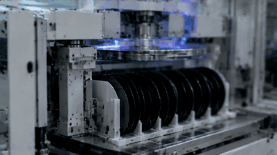
The semiconductor industry is entering a critical transition period as silicon carbide (SiC) technology moves from a specialized material platform toward broader commercial adoption. Once considered an expensive alternative semiconductor material, SiC is rapidly gaining importance in electric vehicles, renewable energy systems, industrial power equipment, and high-efficiency power electronics. A major factor determining the speed of adoption will be the continued decline of SiC substrate costs.

Tracking Expansion Plans of Japan’s Semi Material Giants: Sumitomo, Mitsubishi, Shin-Etsu
Michael Carter
Japan’s semiconductor materials sector has long been a quiet powerhouse beneath the global chip industry. From wafers and photoresists to specialty gases, CMP consumables, and packaging materials, Japanese firms anchor critical parts of the supply chain for fabs worldwide. Among these firms, Sumitomo, Mitsubishi, and Shin Etsu stand out as “semi material giants” whose strategies and expansion plans shape both regional ecosystems in Japan and global availability of key inputs.

Critical Localized Components for Gas Delivery Systems
Alexander Collins
In modern semiconductor fabs, high purity gases are as essential as wafers and photoresists. They feed etch tools, deposition chambers, cleans, and many specialized processes that define device performance and yield. Behind every gas line in the fab is a complex gas delivery system, built from numerous components that must maintain purity, control flow precisely, and ensure safety in an environment where even parts-per-billion contamination can matter. As regions pursue semiconductor localization, attention increasingly turns to “critical localized components” within these gas delivery systems. Localizing these elements is central to building resilient, self-sufficient manufacturing ecosystems.

Volume and Purity Upgrades of Electronic-Grade NaOH in Cleaning Processes
Daniel Foster
The semiconductor industry is entering a period of unprecedented manufacturing complexity as advanced chips, artificial intelligence processors, automotive semiconductors, and high-performance computing applications continue driving demand for higher-quality production processes. Among the many materials required for semiconductor fabrication, electronic grade sodium hydroxide (NaOH) has become an increasingly important chemical component in wafer cleaning and surface treatment processes.
Wet Chemicals’ Purity Leap from G4 to G5 – Domestic Breakthrough Imminent
Andrew Wilson
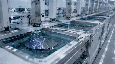
In semiconductor manufacturing, wet chemicals are often described as “silent enablers”. They do not appear in headlines like lithography scanners or etch tools, yet they touch almost every wafer in the fab—during cleaning, surface preparation, etching, stripping, and post-CMP processes. As device dimensions shrink and process windows tighten, the purity requirements on these wet chemicals rise dramatically. The industry’s move from G4-grade to G5-grade purity represents not just an incremental improvement in specifications, but a fundamental leap in how chemical supply, analytics, and process integration are conceived. Domestic breakthroughs in achieving and immersing fabs in G5 wet chemical ecosystems are now a key storyline in localization and yield enhancement.

The Irreplaceability and Supply Risks of High-Purity Quartz in Monocrystal Pulling
David Bennett
High purity quartz is one of those quietly indispensable materials that sit at the foundation of modern semiconductor manufacturing. In monocrystalline silicon pulling—whether via the Czochralski (CZ) process or related techniques—quartz components shape, contain, and protect the molten silicon from contamination and structural defects. Without reliable access to ultra‑clean quartz crucibles and related parts, the global wafer supply chain would struggle, regardless of how advanced lithography, etch, or deposition tools become.

2026 Semi Material Sub-Segment Growth Ranking: Precursors vs. Photoresist vs. Targets
Ethan Parker
In 2026, the semiconductor materials landscape is being reshaped by the push toward advanced nodes, 3D architectures, and regional localization of supply chains. Within this broad shift, three sub segments stand out as critical and fast‑moving: ALD/CVD precursors, photoresists and related lithography materials, and sputtering targets for interconnects and specialty films. Comparing their growth trajectories offers insight into where capital, innovation, and strategic focus are converging across the materials ecosystem.

Soaring Demand for SOI Substrates in RF and Power Devices
Daniel Morgan
Silicon-on-insulator (SOI) technology has moved from a niche substrate option to a strategic pillar in modern semiconductor design, particularly for radio-frequency (RF) and power devices. As smartphones, 5G infrastructure, connected vehicles, and advanced power management systems proliferate, the performance and integration demands placed on RF front-ends and power stages have intensified. SOI substrates, with their unique electrical and isolation characteristics, are increasingly seen as the ideal foundation for meeting these requirements. The result is a pronounced surge in demand for SOI across multiple device categories and applications.

A Complete Map of "Small and Beautiful" Hidden Champions in Semi Materials
David Mitchell
The semiconductor industry is often associated with famous chip designers, leading foundries, and advanced equipment manufacturers. Companies developing processors, memory chips, and lithography systems frequently receive global attention because their products directly influence technology trends. However, behind every advanced semiconductor device exists a complex ecosystem of specialized material suppliers that quietly enable the entire industry.

Certification Barriers and Breakthrough Cases for Chinese Material Firms Entering Global Supply Chains
Lucas Bennett
The global semiconductor industry is undergoing a major transformation as supply chains become more diversified, regionalized, and strategically important. Semiconductor materials, once considered a relatively stable part of chip manufacturing, have become one of the most critical competitive areas in the industry. For Chinese semiconductor material companies, entering global supply chains represents both a significant opportunity and a complex challenge. While China has developed strong capabilities in many material segments, gaining acceptance from international semiconductor manufacturers requires overcoming strict certification barriers, technological requirements, and long-established supplier relationships.

CMP Pad and Slurry Market Structure: The Moats of DuPont and Cabot
Ethan Richardson
Chemical mechanical planarization (CMP) is one of the most critical yet often understated processes in semiconductor manufacturing. It quietly ensures that wafers maintain the flat, precisely controlled surfaces needed for successive lithography, etch, and deposition steps. At the center of CMP are two indispensable consumables: pads and slurries. Over the past decades, a small group of global players—most prominently DuPont and Cabot—have built strong positions around these products, developing what can fairly be described as “moats” in the CMP pad and slurry market structure.

The Material System Transition of Sputtering Targets (Al/Cu/Ti/Co) in Advanced Interconnects
Henry Cooper
Advanced interconnects have quietly become one of the most challenging frontiers in semiconductor manufacturing. As device performance, power efficiency, and reliability demands tighten at each new logic and memory node, the wiring that connects transistors and functional blocks has evolved just as dramatically as the transistors themselves. Central to this evolution is the material system used in thin-film deposition, especially sputtering targets based on aluminum (Al), copper (Cu), titanium (Ti), and cobalt (Co). The transition in these target materials reflects a broader shift in how the industry manages resistance, electromigration, barrier integrity, and manufacturability in increasingly complex interconnect stacks.

Impact of Germanium/Gallium Export Controls on Semi Material Supply Chains
Ethan Richardson
The semiconductor industry has entered a new era in which material security has become as important as technological innovation. For decades, the global chip industry focused primarily on advancing transistor performance, increasing manufacturing efficiency, and expanding semiconductor capacity. However, recent supply chain disruptions and geopolitical tensions have highlighted a critical reality: access to specialized materials can determine the stability and competitiveness of the entire semiconductor ecosystem.

New Application Scenarios of Silicon-Based Materials in 3rd-Gen Semi Substrates
Andrew Wilson
Third-generation semiconductor substrates such as silicon carbide (SiC) and gallium nitride (GaN) are reshaping power electronics, RF devices, and high‑efficiency energy systems. They are often described as a break from traditional silicon, yet silicon‑based materials have not disappeared from the picture. Instead, they have found new, strategically important roles around these wide‑bandgap substrates: as templates, integration platforms, thermal and mechanical partners, and key elements in hybrid packaging. The interplay between silicon and third‑generation semiconductors is becoming a central theme in how next‑generation devices are designed and manufactured.

Empirical Analysis of Price Transmission from Material to Foundry End
David Mitchell
The semiconductor industry is built upon one of the most complex and interconnected supply chains in the global manufacturing economy. From raw materials and specialty chemicals to semiconductor equipment, wafer fabrication, packaging, and final electronic products, each stage influences the economics of the entire value chain. Among these relationships, the transmission of price changes from semiconductor materials to foundry manufacturing costs has become an increasingly important topic as the industry experiences supply shortages, capacity expansions, and technology transitions.

2026 Photoresist Localization Target of 20%: Which Companies Benefit Most?
Henry Cooper
The semiconductor industry is entering a period of accelerated transformation as countries and companies increasingly focus on supply chain security, technological independence, and domestic manufacturing capabilities. Among the many semiconductor materials requiring localization, photoresists have become one of the most strategically important categories due to their direct impact on lithography performance, wafer yield, and advanced semiconductor production.

Materials Segment’s Elasticity Coefficient Far Exceeds Design Segment in Upswing
Richard Evans
When the semiconductor industry enters an upswing, not all segments respond in the same way. Revenue and profit growth in chip design, manufacturing, equipment, and materials move at different speeds and magnitudes. One of the most striking patterns observed across cycles is how strongly materials segments react compared with the design segment: their “elasticity coefficient” with respect to industry upturns often far exceeds that of design. Put simply, when the cycle turns up, materials businesses frequently grow faster and more sharply than fabless design houses, even though both benefit from rising demand.

The Price Spread and Capacity Bottlenecks Between EUV and ArF Photoresists
Nathan Foster
The semiconductor industry has entered an era where advanced manufacturing is no longer limited only by transistor design, lithography machines, or wafer fabrication capacity. Increasingly, the availability, pricing structure, and production scalability of key process materials have become critical factors determining the pace of semiconductor innovation. Among these materials, photoresists occupy a strategically important position because they directly influence the precision, yield, and economic efficiency of semiconductor patterning.

Electronic Specialty Gas Usage Surges in Advanced Nodes, Localization Accelerates
Daniel Brooks
As semiconductor manufacturing pushes deeper into advanced logic and memory nodes, electronic specialty gases have shifted from supporting materials to central enablers of critical processes. Their usage has surged in volume, diversity, and technical importance, particularly in front-end steps such as etch, deposition, doping, and chamber conditioning. At the same time, localization of specialty gas supply—developing domestic or regional production capabilities rather than relying heavily on global imports—has accelerated across multiple semiconductor hubs.

Wafer Size Battle: 300mm Demand Share Continues to Rise, 200mm Stabilizes
Ethan Parker
The semiconductor industry has always been defined by continuous technological advancement, and wafer size evolution remains one of the most important drivers of manufacturing efficiency. Over the past two decades, the transition from 200mm wafers to 300mm wafers has reshaped semiconductor production economics by enabling higher output, improved cost efficiency, and greater manufacturing scalability. As global demand for advanced computing, artificial intelligence, automotive electronics, and industrial semiconductors continues to expand, the balance between 300mm and 200mm wafer demand is becoming a critical topic across the semiconductor supply chain.

Photomask Localization Rate Breaks Through – Progress by Qingyi and Luwei
Alexander Morgan
In the semiconductor world, photomasks sit at a critical junction between design data and physical wafers. They encode circuit patterns with nanometer precision and serve as the optical templates for lithography across logic, memory, and specialty devices. For years, high-end photomask capability has been concentrated in a handful of global clusters, making domestic fabs heavily dependent on imported masks for advanced nodes. Recently, however, localization rates in certain regions have begun to break through, driven by progress from emerging players such as Qingyi and Luwei. Their advances mark a significant shift in the balance between global and domestic supply and signal a new phase in the maturation of local semiconductor ecosystems.
Material Inventory Cycles Typically Lead Equipment Inventory by 1-2 Quarters
Matthew Collins
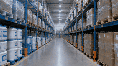
The semiconductor industry operates through one of the most complex supply chains in the global manufacturing ecosystem. From raw materials and specialty chemicals to semiconductor equipment and final chip production, every stage is closely connected through demand signals, inventory adjustments, and capital investment cycles. Understanding the relationship between material inventory cycles and equipment inventory cycles provides important insight into the future direction of semiconductor markets.

Photoresist Supplier Price Hike Wave: Shin-Etsu and JSR’s Strategy Shifts in China
Thomas Walker
Photoresist sits at the heart of semiconductor manufacturing. As a key material in lithography, it directly shapes how patterns are transferred onto wafers and, ultimately, how advanced devices are made. In recent years, China has emerged as one of the most important semiconductor markets, both as a manufacturing base and as a consumer of critical materials like photoresist. Against this backdrop, a wave of price hikes by major suppliers—and evolving strategy from global leaders such as Shin Etsu and JSR—has become a focal point for fabs, policymakers, and industry observers trying to understand the changing economics of chipmaking in China.
Precursor Demand Explodes in ALD/CVD – Korean Suppliers Dominate
Alexander Morgan
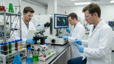
As semiconductor manufacturing races into ever more advanced nodes and complex device architectures, atomic layer deposition (ALD) and chemical vapor deposition (CVD) have become foundational processes for building precision films and 3D structures across logic, memory, and advanced packaging. With this shift, demand for electronic-grade precursors—the reactive molecules that form these films—has exploded. At the same time, Korean chemical and materials companies have steadily expanded their footprint, to the point where they now play a dominant role in supplying key ALD and CVD precursors to global fabs.

Recycling and Circularity of Semi Materials (Green Silicon) as an ESG Investment Theme
Daniel Foster
Semiconductor manufacturing sits at the crossroads of technological progress and environmental scrutiny. As demand for chips soars—driven by AI, mobile devices, electric vehicles, and IoT—so do the material flows, energy consumption, and waste streams that underpin fabrication. "Green silicon" and broader circular approaches for semiconductor materials are emerging as crucial elements of environmental, social, and governance (ESG) investment strategies. This article explains why recycling and circulation of semiconductor materials matter, outlines the main technical and market levers, highlights key risks and opportunities for investors, and offers practical frameworks for integrating these themes into ESG-focused portfolios.

Why Semi Material Suppliers Generally Have Higher Gross Margins than Equipment Makers
Michael Foster
Within the semiconductor ecosystem, two groups of companies are structurally critical: equipment makers that build the tools used in fabrication, and material suppliers that provide wafers, gases, chemicals, photoresists, targets, and numerous other inputs. Although both operate in demanding, capital‑intensive environments, semi material suppliers typically achieve structurally higher gross margins than equipment manufacturers. This outcome can seem counterintuitive at first glance—tools are expensive and complex—but it makes sense once you examine business models, product lifecycles, and the nature of recurring demand.