
Equipment

Wafer Fab Equipment Spending Forecast 2026: SEMI’s Upward Revision to $152B
James Wilson
The semiconductor equipment outlook has strengthened substantially, but the number attached to that improvement needs careful handling. The requested $152 billion figure could not be verified as SEMI’s 2026 wafer fab equipment forecast. In its July 2026 equipment sales update, SEMI projected wafer fab equipment sales of $143.9 billion, up 23.1% from 2025, and total semiconductor manufacturing equipment sales of $165.9 billion. Those figures describe different market categories and should not be combined or substituted for one another.

Electrostatic Chucks and Ceramic Heaters: The Core Component Shortage
Kevin Foster
A semiconductor factory can have enough cleanroom space, a healthy equipment budget, and strong customer demand—and still struggle to add productive capacity. Sometimes the missing link is not a complete machine. It is a highly specialized component that holds a wafer in place or controls its temperature inside a process chamber.

Advanced Packaging Equipment Growth: Outpacing Front-End Tools
Lucas Anderson
The traditional division of semiconductor manufacturing was easy to describe. Front-end fabs created devices on wafers; back-end providers assembled, packaged, and tested them. Equipment purchasing broadly followed the same boundary. A foundry bought deposition chambers and etchers, while an assembly operation bought bonders, molders, and test systems.

TSMC’s 20 Fabs Under Construction: The Equipment Order Pipeline
Andrew Mitchell
TSMC’s construction activity is becoming a defining signal for semiconductor equipment demand. When the world’s largest contract chipmaker develops multiple manufacturing projects simultaneously, the consequences extend beyond concrete, cleanrooms, and regional investment announcements. Each project creates requirements for process tools, subsystems, installation teams, and continuing service.

Advanced Ceramic Components in Etch and Deposition: The <10% Localization Gap
Charles Wilson
A semiconductor equipment company can assemble a competitive etch or deposition platform while remaining dependent on overseas suppliers for several of its most important internal components. The chamber carries a domestic brand, the controls are developed locally, and the process has passed customer evaluation. Yet the ceramic parts exposed to plasma, heat, and demanding chemistry may still come from a narrowly qualified supplier base.

China’s Equipment Localization Rate at 55%: The Mature Node Milestone
Daniel Morgan
A semiconductor factory can become substantially more local without becoming entirely independent. Domestic etch chambers may operate alongside imported lithography systems. A locally assembled deposition tool may still rely on overseas components. An expanding packaging operation may use a different supplier mix from the wafer fab feeding it.
Ceramic Component Localization: The 10% to 30% Path
Ryan Mitchell
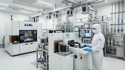
A ceramic component rarely becomes the public face of semiconductor manufacturing. It does not carry the recognition of a lithography scanner or the commercial excitement of an AI accelerator. Yet inside a process chamber or power-device package, it can determine whether equipment operates consistently and whether a finished device survives its intended conditions.

Lam Research’s Extended Lead Times: Etch and Deposition Equipment at 12 Months
Richard Morgan
A twelve-month wait for semiconductor equipment changes more than a purchasing schedule. It changes when a fab can add capacity, how customers reserve manufacturing resources, and how suppliers organize production. For etch and deposition systems, that delay can sit directly on the critical path between a technology roadmap and commercial output.

ASML’s High-NA EUV Triple Partnership: Intel, Samsung, TSMC’s Production Plans
Jonathan Reed
High-numerical-aperture extreme ultraviolet lithography is moving from an engineering development into a manufacturing roadmap shared by the industry’s largest chipmakers. The transition is not happening on one schedule, however, and the commercial implications depend on recognizing those differences.
Vacuum Pump and RF Generator Shortages: The Equipment Sub-Component Bottleneck
Alexander Morgan
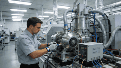
A semiconductor production tool can be almost finished and still be commercially useless. The chamber is assembled, the automation works, and the customer has prepared an installation slot. Yet one missing vacuum pump or radio-frequency power subsystem can prevent the equipment from completing its final tests and leaving the factory.

Applied Materials’ FY26 Q4 Revenue Beat: The Equipment Supercycle Evidence
Michael Evans
Applied Materials’ fiscal 2026 fourth-quarter revenue beat cannot yet be evaluated as a completed event. As of October 9, 2026, the company’s latest reported quarter was fiscal Q3, and its investor presentation listed November 12 as the projected date for its Q4 earnings call. What exists today is a strong reported quarter and an ambitious forward outlook—not an announced Q4 result.

Equipment Order Backlog Visibility: Why 2027 Deliveries Are Already Booked
William Turner
For selected semiconductor equipment suppliers, 2027 is already taking shape inside the order book. Customers are reserving systems before the delivery year begins, manufacturers are allocating production capacity, and component suppliers are preparing for schedules that extend beyond the next quarterly earnings report.

Order Visibility vs. Valuation Matching Analysis for Semi Equipment Stocks
Matthew Foster
Semiconductor equipment stocks sit at the crossroads of technology cycles and capital markets. Their revenues are tied to wafer‑fab and packaging investments, yet their valuations reflect investors’ expectations about future demand, competitive positioning, and macro risk. One of the most important lenses for understanding these stocks is the relationship between order visibility—how far into the future companies can see and quantify demand—and the valuations assigned to them.

New Applications of High-Energy Ion Implantation in SiC Power Devices
Daniel Walker
Silicon carbide (SiC) has become one of the most important wide bandgap semiconductors for next‑generation power electronics, thanks to its ability to handle high voltages, high temperatures, and fast switching with relatively low losses. As SiC devices move deeper into electric vehicles, renewable energy systems, industrial drives, and data center power supplies, process technologies around SiC must evolve to unlock the full potential of the material. High energy ion implantation is one of those enabling technologies, and its role is expanding beyond conventional doping to a wider range of applications within SiC power devices.

Localization Progress of Equipment Parts: Ceramic Heaters and Electrostatic Chucks
Daniel Walker
As semiconductor manufacturing becomes more strategically important and supply chains more scrutinized, attention is shifting from headline tools—like lithography scanners and etchers—to the critical parts inside these systems. Among the most important of these parts are ceramic heaters and electrostatic chucks, which play central roles in thermal management and wafer handling in front‑end processes. Their localization, meaning the development and production of these parts within domestic or regional ecosystems rather than relying entirely on imports, is now a key topic for both equipment vendors and fabs.

Consumables Business Model and Valuation Premium of CMP Equipment
Alexander Reed
Chemical mechanical planarization (CMP) is one of the quiet but indispensable steps in semiconductor manufacturing, ensuring that wafers remain flat and ready for subsequent patterning and deposition. CMP equipment vendors occupy a distinctive position in the fab tool ecosystem because their business model is tightly linked to consumables—slurries, pads, conditioners, and related materials that must be replenished continuously.

The Decisive Role of Dual-Stage Systems in Lithography Overlay Accuracy
Ethan Mercer
As semiconductor manufacturing has pushed deep into advanced logic and memory nodes, overlay accuracy has become one of the most critical metrics in lithography performance. Overlay—the precise alignment of a new pattern layer to all the layers already on the wafer—directly determines whether transistors, contacts, and interconnects line up within the extremely tight tolerances required at nanometer-scale dimensions. At these nodes, even a few nanometers of misalignment can translate into yield loss, parametric variability, or outright functional failures.

Challenges for Back-End Test Equipment (Probers/Handlers) in Massive AI Chips
Andrew Wilson
Massive AI chips—large, power‑hungry accelerators packed with billions of transistors and complex interconnect fabrics—have rapidly become central to data centers, cloud platforms, and high‑performance computing systems. Their front‑end design and fabrication attract much attention, but back end test is just as critical. Probing and handling these devices at wafer sort and final test is significantly more challenging than for traditional logic or consumer chips, because AI devices push the limits of size, power, thermal behavior, and interface complexity.
ALD Usage Doubles in Advanced Process Nodes
Ethan Richardson
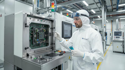
Atomic layer deposition (ALD) has moved from a niche technique to a central pillar of thin-film engineering in leading-edge semiconductor manufacturing. As process nodes advance into ever smaller geometries and more complex three-dimensional architectures, fabs are turning to ALD far more frequently than in previous generations. The statement that “ALD usage doubles in advanced process nodes” captures a real and powerful trend: each node shrink and structural transition typically brings a step-change in how often, and how critically, ALD is used across the flow.

2026 Global Semi Equipment Market Forecasts: A Summary of Institutional Divergence
Richard Evans
The 2026 global semiconductor equipment market sits at the intersection of multiple, sometimes conflicting forces: post-downturn recovery, structural demand from AI and automotive, technology transitions at advanced nodes, and ongoing geopolitical constraints. Institutions that track and forecast this market—industry associations, research houses, banks, and policy bodies—do not agree on a single trajectory. Instead, their forecasts diverge along several axes: size of the rebound from recent softness, sustainability of capital expenditure cycles, and the regional composition of spending.

Edge Polishing Equipment Opportunities in Growing SOI Substrate Demand
Christopher Reed
Silicon-on-insulator (SOI) substrates have moved from a niche technology into a mainstream enabler for high‑performance, low‑power, and high‑voltage semiconductor devices. As adoption expands in RF, automotive, power management, and advanced logic applications, demand for SOI wafers is rising steadily. This growth is not just about the active silicon layer and buried oxide quality; it also places new emphasis on wafer edge characteristics, opening a distinct opportunity space for specialized edge polishing equipment.

Shortage Cycles of Semi Equipment Components (RF Generators, Vacuum Pumps, Ceramics)
Thomas Walker
Semiconductor equipment may command the headlines, but behind every etcher, deposition tool, or plasma cleaner sits a network of critical components that quietly determine whether fabs can actually run at full capacity. RF generators and matching networks power plasmas, vacuum pumps sustain clean low‑pressure environments, and ceramic parts protect chambers while withstanding extreme conditions. When these components fall into shortage, the impact cascades through tool delivery schedules, fab utilization, and ultimately chip supply.
Inspection/Metrology Tools Become the Key Lever for Yield Improvement
Christopher Reed
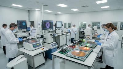
As semiconductor manufacturing pushes deeper into advanced nodes, 3D architectures, and heterogeneous integration, yield has become both harder to achieve and more critical to economic success. Traditional levers for yield improvement—recipe tuning, equipment maintenance, and operator experience—are no longer sufficient on their own. Today, inspection and metrology tools have emerged as the key lever for yield enhancement, providing the data, visibility, and control needed to manage processes at nanometer scales and across complex three‑dimensional structures.

Short-Term Impact Assessment of Japan Earthquakes on Global Equipment Supply Chain
Christopher Reed
Japan sits at the heart of the global semiconductor equipment ecosystem. It is home to critical tool makers, key sub‑component suppliers, specialty materials vendors, and precision manufacturing firms that support fabs worldwide. When significant earthquakes hit Japan, the immediate concern for the semiconductor industry is not only human safety and local infrastructure damage, but also the short‑term impact on equipment and parts supply. Even relatively brief disruptions in Japanese production or logistics can ripple through global tool delivery schedules, fab ramp plans, and maintenance activities.
Coat/Develop Equipment Localization Rate First Breaking 30% – Industry Significance
Michael Evans
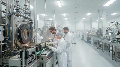
The lithography track—specifically coat and develop equipment—has long been one of the most strategically sensitive segments of semiconductor manufacturing. For years, a small number of global suppliers dominated this space, providing the photoresist coating and developing tools that sit directly alongside lithography scanners and define patterning quality and throughput. The news that localization rates for coat/develop equipment have, for the first time, broken through the 30% threshold is therefore more than a statistical milestone. It represents a meaningful shift in technological capability, supply‑chain security, and bargaining power across the industry.

2026 Semi Equipment Localization Targets and Their Capital Market Reflections
Robert Carter
Semiconductor equipment localization moved from a long‑term aspiration to an explicit 2026 policy target in many key manufacturing regions. Governments and industry coalitions have set concrete goals for the share of critical tools—lithography tracks, etch and deposition systems, metrology instruments, back‑end and packaging equipment—that should be sourced from domestic or regional suppliers. These targets are not only reshaping procurement strategies inside fabs; they are also sending clear signals to capital markets, where investors sift through winners and losers in the emerging localized equipment ecosystem.

Advanced Packaging Equipment Growth Outpaces Front-End Equipment for the First Time
Richard Evans
For decades, the center of gravity in semiconductor capital spending has lived squarely in the front end of the line—lithography, etch, deposition, and other wafer‑fab tools. Packaging was often treated as an afterthought: necessary, but secondary. That hierarchy is now changing. For the first time, growth in advanced packaging equipment is outpacing growth in traditional front end equipment, signaling a structural shift in how performance, cost, and innovation are created in the chip industry.

2026 Breakthroughs in Lithography Supply Chain Localization: A Critical Component Progress List
James Wilson
In 2026, efforts to localize the lithography supply chain—once seen as an almost impossible task—have begun to show tangible progress. Lithography, the core process technology enabling advanced semiconductors, has long depended on a small set of suppliers for key tools and materials. This concentration created geopolitical vulnerability, bottlenecks, and strategic concerns for countries and regions that rely heavily on imported equipment and components. Over the past year, multiple initiatives have focused on building domestic capabilities and diversifying sources for critical lithography inputs.

The Critical Role of Etching Equipment in 3D NAND’s 500-Layer Breakthrough
Jonathan Brooks
The push toward 500‑layer 3D NAND marks one of the most ambitious feats in modern semiconductor manufacturing. As vendors stack more layers to drive bit density and lower cost per bit, the process challenges grow exponentially rather than linearly. At the center of these challenges sits etching equipment. While lithography and deposition often capture headlines, it is the precision, selectivity, and reliability of advanced etchers that make ultra‑tall vertical structures physically realizable at scale. Without breakthroughs in etching technology, a 500‑layer architecture would remain a simulation rather than a shipping product.
Global Wafer Shipment Area Stabilizes and Rebounds – Equipment Inflection Confirmed
Michael Evans
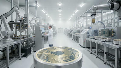
After several volatile years in the semiconductor cycle, global wafer shipment area has finally moved from contraction to stabilization and, more recently, to a clear rebound. This turning point is more than a statistical curiosity: it signals a broad‑based recovery in chip demand and a renewed appetite for equipment investment. As wafer area shipped stabilizes and then climbs, the reflection in front‑end manufacturing equipment orders and utilization is becoming unmistakable, confirming that the industry has entered a new phase of expansion.

Equipment Makers Transition from Hardware Sales to "Hardware + Service + Consumables" Model
Matthew Foster
Semiconductor manufacturing has long been defined by massive capital investments in complex tools: lithography scanners, etchers, deposition systems, implant machines, metrology platforms, and packaging equipment. For decades, the core business of most equipment makers revolved around selling this hardware—large, one‑time transactions that anchored fab capacity expansion and technology upgrades. Today, that model is undergoing a decisive transformation. Across the industry, equipment makers are shifting from pure hardware sales toward integrated “Hardware+Service+Consumables” offerings, where long‑term support contracts, process services, and recurring consumable sales form an increasingly large share of revenue and strategic focus.

Wet Cleaning Tools’ Share of Process Steps Continues to Rise in Advanced Nodes
Alexander Morgan
As semiconductor manufacturing has pushed into ever more advanced nodes, wafer cleaning has evolved from a supporting operation into one of the central pillars of yield and device performance. At leading logic and memory nodes, the share of total process steps devoted to cleaning tools—single-wafer cleans, batch cleans, bevel cleans, and specialized surface treatments—continues to rise. This expansion reflects a simple reality: smaller geometries, complex three-dimensional structures, and new materials leave far less margin for particles, residues, and surface defects, making cleaning an indispensable, frequently repeated step throughout the flow.

Why Semi Equipment ETFs Continue to Outperform Foundry ETFs – A Deep Attribution Analysis
Benjamin Harris
In recent years, exchange‑traded funds (ETFs) focused on semiconductor equipment makers have tended to outperform those centered on foundries and chip manufacturers. This pattern has persisted across multiple market cycles, surprising some investors who assume that the companies producing finished chips should capture the greatest share of value. A closer look reveals that equipment makers occupy a structurally advantaged position in the semiconductor ecosystem, translating into relatively resilient earnings, powerful operating leverage, and compelling long‑term growth narratives.

Seasonality Patterns in Equipment: Q4 Typically the Order Peak
James Carter
Semiconductor equipment demand is anything but random. Over decades of industry development, a recognizable rhythm has emerged in how chipmakers and foundries place orders for tools such as lithography scanners, etchers, deposition systems, and testers. One of the most persistent features of this rhythm is seasonality: fourth quarter (Q4) often emerges as the peak period for equipment orders, with the rest of the year showing more mixed patterns.
2026’s Biggest Variable for Equipment Localization: Complete Lithography System Progress
Matthew Collins
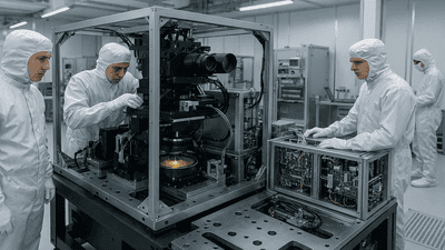
In semiconductor manufacturing, “equipment localization” has become a central strategic goal for many countries: building domestic or closely allied capability to produce and maintain the tools that make chips. Across etch, deposition, cleaning, test, and packaging, notable progress has been made. Yet in 2026, one segment still stands out as the biggest variable in localization efforts: complete lithography systems. Lithography remains the technical and strategic bottleneck, and the pace of progress toward localized, fully integrated lithography platforms will largely determine how far and how fast equipment localization can go.

The Leap from 20% to 50% Localization – Ranking the Beneficiaries Across Segments
Jonathan Mercer
Semiconductor localization has moved from abstract policy talk to concrete numerical targets. Many countries and regions now speak explicitly about raising the local share of their semiconductor value chain—from 20% toward 50% or more—across materials, equipment, design, and manufacturing. This leap is not incremental; it fundamentally changes how risks, costs, and strategic advantages are distributed in the ecosystem.

Oligopoly Structure of the Ion Implanter Market and China’s Breakthrough Opportunities
Matthew Collins
Ion implanters sit at the core of modern semiconductor manufacturing, enabling precise doping of silicon and other substrates to form the active regions of transistors and memory cells. Over decades, this highly specialized equipment segment has evolved into a tight oligopoly dominated by a handful of global vendors with deep process know‑how, sophisticated engineering capabilities, and entrenched customer relationships. For new entrants, especially those in emerging technology powers like China, this structure presents both formidable barriers and compelling strategic opportunities.

Thin Film Deposition Tools (PVD/CVD/ALD) See Surging Demand, Orders Booked into 2027
Ryan Carter
Thin film deposition sits at the core of modern semiconductor manufacturing, quietly shaping every transistor, interconnect, and memory cell. As chips become more complex and vertically integrated, the demand for high‑performance deposition equipment—especially physical vapor deposition (PVD), chemical vapor deposition (CVD), and atomic layer deposition (ALD)—has accelerated. In recent cycles, this demand has reached the point where order books for key tools are being filled well into 2027, signaling both a structural shift in capital expenditure and a sustained confidence in long‑term semiconductor growth.

Assessing the Impact of 2026 New US Export Controls on Equipment to China
Alexander Morgan
The semiconductor industry entered 2026 already shaped by several years of tightening technology and trade restrictions, and new US export controls on equipment shipments to China add another layer of complexity. These measures aim to constrain China’s access to advanced manufacturing capabilities, particularly for leading‑edge logic, memory, and certain specialty devices that have strategic or military relevance. For companies operating fabs, supplying tools, or sourcing equipment in China, the question is not whether these controls matter—they clearly do—but how their impact will differ across segments, time horizons, and strategic options.

Booming Used Equipment Market – An Alternative Path for Mature Node Capacity Expansion
Nathan Collins
As global demand for semiconductors at mature process nodes continues to grow, chipmakers face a strategic question: how to expand capacity without committing to the full cost and lead time of brand‑new fab tooling. In this environment, the used semiconductor equipment market has shifted from a niche corner of the industry into a booming, mainstream alternative. Buying, refurbishing, and redeploying used tools has become a key path for adding mature node capacity quickly and economically, reshaping investment decisions and competitive dynamics across the ecosystem.
Rising Penetration of Equipment Leasing Models Among China’s Small-to-Mid Fabs
Charles Foster
Small and mid‑sized semiconductor fabs in China are under intense pressure to expand capacity, upgrade technology, and remain competitive, all while facing tight capital budgets and a rapidly changing market landscape. The traditional model of buying expensive front‑end and back‑end equipment outright is increasingly difficult to sustain for these fabs, especially when technology lifecycles are shortening and demand cycles remain volatile. In this environment, equipment leasing and related flexible acquisition models are gaining traction as practical solutions.

A Side-by-Side Comparison of 2026 Guidance from ASML, AMAT, LRCX, and TEL
Robert Carter
Guidance for 2026 from the four global leaders in semiconductor equipment—ASML, Applied Materials (AMAT), Lam Research (LRCX), and Tokyo Electron (TEL)—offers a window into how each is positioned for the next phase of the wafer fab and advanced packaging cycle. While the numerical details differ, the guidance sets share common themes: strong demand tied to AI and advanced nodes, resilient spending on mature and specialty technologies, and varying degrees of caution around geopolitics and export controls.